This time two years ago, we published a blog on the inconsistent terminology used to describe an AFM probe (AFM tip, AFM cantilever, etc). This inconsistency is not unique to how AFM probes are named but also rears its ugly head within the AFM community when their properties are discussed.
As AFM users, we generally accept that the sharper the tip of an AFM probe, the higher the resolution of our image. But what do we actually mean when we talk about tip sharpness?
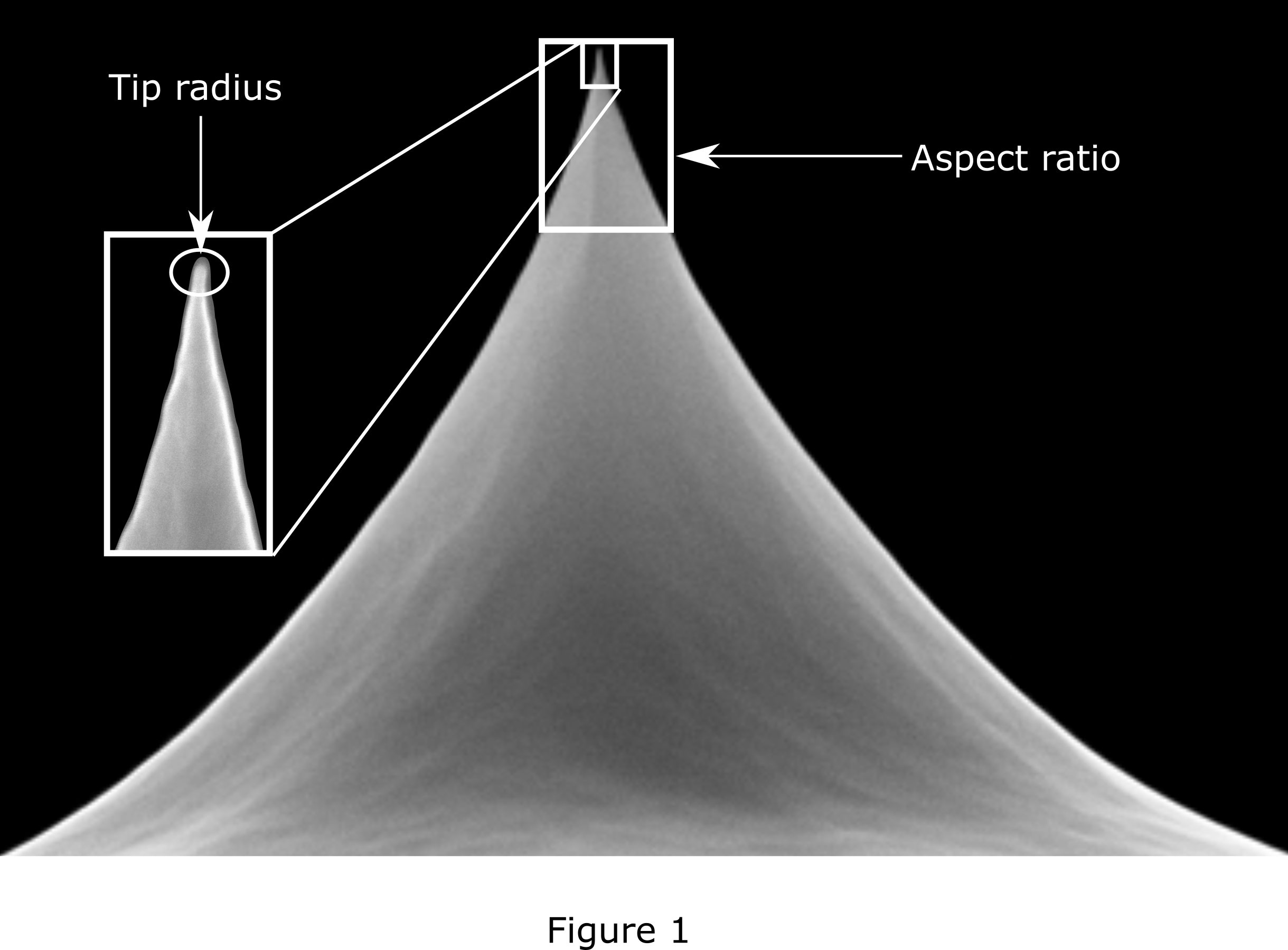
In fact, it is often used to describe two separate properties of an AFM probe: the radius of curvature of the tip apex (hereafter, the tip radius) and the aspect ratio of the tip (the ratio between its height and width), as shown in Figure 1, which represent sharpness at two different scales, the nano- and micro-scale, respectively.
To improve imaging resolution, it is important to understand the difference between the tip radius on the nano-scale and tip aspect ratio on the micro-scale. In doing so, the effects of these two properties must be considered in the context of the specific sample surface under study.
Tip radius:
When an AFM tip scans over the sample surface, the tip radius needs to be smaller than the size of the surface features in order to resolve them. As shown in Figure 2 (a) below, a tip with a radius of curvature smaller than the surface features traces out the topography of the surface more accurately because the tip apex is able to scan over each point of the feature.
However, as shown in Figure 2 (b), when the probe tip has a radius larger than the size of the surface features, the features will appear larger than their actual size in the acquired image. Furthermore, if two features are spaced close together, the probe may resolve them as one large feature.

Aspect ratio:
A high aspect ratio AFM tip is particularly useful in situations where the features of the sample surface have steep sidewalls or edges such as trenches, which are common in semiconductor device processing. This is because the height and width of the tip will be larger and smaller than the depth and width between the sidewalls of the trench, which allows the tip apex to scan along the sidewalls and bottom of the trench, as shown in Figure 3 (a) below.
In the case of a lower aspect ratio tip, its apex does not extend to the bottom of the trench. In this case, the feature is imaged as narrower and shallower than its real profile, as seen in Figure 3 (b).
High aspect ratio is generally achieved by removing part of the tip sidewalls via etching or ion beam milling. The depth of such trenches is commonly around 1 µm so high aspect ratio typically only needs to be achieved in the region of the tip extending from the apex to a distance slightly greater than the depth of the trench.

In summary, tip radius determines absolute imaging resolution at the nanometre or even sub-nanometre scale and aspect ratio governs the ability to resolve highly three-dimensional structures or features with steep edges.
So, a New Year’s resolution for you: when you are considering which AFM probe to choose for imaging your sample, consider the expected dimensions and topography of its surface features. This will determine whether a tip with a smaller tip apex radius or high aspect ratio is more relevant for your work.
If you liked this blog post, you may also like From one AFM user to another..., (Nearly) Everything you ever wanted to know about AFM but were afraid to ask…, and 5 top tips for effective AFM imaging: a beginners guide.