How frustrating is it to have spent time carefully preparing your sample and setting up the AFM only to find that you’re not getting the images you expected?
Having problems acquiring accurate images is incredibly common, especially if working with the AFM is reasonably new to you.
In most instances it will be due to one of three main things - your sample, the probe you’re using, or because someone else has fiddled with the AFM default settings.
To help navigate some of the common causes of imaging problems you may come across we’ve compiled a short and simple guide of the main problems, what causes them and how you can fix them.
1.
Problem: Unexpected patterns in images
Cause: Tip artefacts
Structures appearing duplicated or irregular shaped features repeating across the image can indicate a broken tip or contamination on the tip. With a blunt tip, structures will appear larger and trenches will appear smaller. If you are seeing either of those things try using a new probe to see if that makes the problem disappear. At NuNano we understand this frustration first hand! We inspect every probe to guarantee tip sharpness, to ensure no contaminated or broken probes which could produce unexpected shapes.
AFM Image showing duplicate features, taken from: Lamentation of Arti(e)facts - 2020 - Wiley Analytical Science
For some more information on probe artefacts, take a look at this blog on ‘Lamentation of Arti(e)facts’ by Dalia Yablon and Philip Moriarty in Microscopy & Analysis: https://analyticalscience.wiley.com/do/10.1002/was.00020100
2.
Problem: Difficulty imaging vertical structures and/or deep trenches
Cause A: Side-wall from pyramidal or tetrahedral shaped probe
Particularly with samples with high aspect ratio features you may be using the wrong type of probe. Check which probe you are using including what shape it is. Conical tips are superior to pyramidal and tetrahedral types in many ways. They can be fabricated with higher aspect ratio (because etching along a particular crystal orientation is not required for their fabrication). As you can see from the image below the trace of a conical tip over a surface with steep-edged features more closely resolves the “real” profile of this surface.

(a) A conical tip

(b) A tetrahedral tip
Read more in our AFM guide: The superiority of conical tips in AFM
Cause B: Side-wall from low aspect ratio probes
The aspect ratio is defined as the ratio between the height and width of an AFM tip. Conventional probes are unable to accurately resolve the topography of highly non-planar features such as deep and narrow trenches, common in semiconductor device processing. The tip apex is unable to reach the bottom of the trench. Using HAR probes with high aspect ratio tips would resolve this issue as they can fit inside the trenches and produce high-resolution images of these types of features as shown in the image below.


Read more about the benefits of an HAR tip in our AFM guide: Improving image resolution with high aspect ratio (HAR) atomic force microscopy (AFM) probes
3.
Problem: Repetitive lines appearing across the image
Cause A: Electrical noise.
Electrical noise is easiest to identify first, since its frequency is likely to be 50 Hz. You can compare the frequency of the noise in the image to the scan rate. If your scan rate is 1 Hz, you will see 25 lines on the image, i.e. 25 lines in the trace direction and 25 lines on the retrace, totalling 50 lines in 1 second (50 Hz). If you halve the scan rate, you should see twice as many lines in the image.
In many cases electrical noise can be out of your control, since it’s likely governed by the quality of the electrical circuits in the building, other instrumentation etc. Sometimes it’s possible to identify periods (e.g. early mornings/late evenings) when this problem doesn’t persist, albeit necessitating a change in working habits…)
Cause B: Interference of the laser reflecting off the sample.
A more common cause is laser inference: On most AFM systems some portion of the laser spot will spill off the sides of the cantilever. If the sample is highly reflective, there may be some reflection of the laser light from the sample surface that enters the photodetector, interfering with the light reflecting off the cantilever. Additional interference can occur with light reflecting off the front (tip) side of the cantilever, since thin cantilevers are semi-transparent to typical wavelengths of the laser.
Using a probe with a reflective coating, typically aluminium or gold, can eliminate both of these problems. The metal coating acts to prevent interference between the primary laser signal and reflected light from other surfaces.

For more information about advantages and drawbacks of reflective coatings, different types of metal coatings, and what coatings should and should not be used download our AFM guide: Reflective coating of the cantilever in atomic force microscopy (AFM)
4.
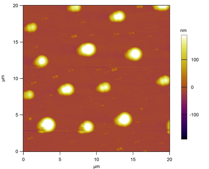
Problem: Streaks on your images
Cause A: Environmental noise/vibration
Environmental vibrations from people moving around the building, open/closing doors, or traffic outside on the street, can affect your images (especially when you’re working on images requiring high resolution). Most AFMs are sold with some form of anti-vibration table and, less commonly, an acoustic box. Make sure the AV table is working, e.g. if it requires a gas supply, it hasn’t run out. Again, carrying out your imaging at a quiet time where possible or even relocating your instrument to a basement room can reduce this.

Sometimes the people around you are simply unaware that there’s vibration sensitive work going on in the lab. We’ve created a ‘STOP AFM in progress’ poster which you’re free to download here. Just letting people know you are imaging a sample could be the easiest and simplest solution. Most fellow researchers will be understanding about your need for them to keep the noise down to decrease chances of noise vibration affecting your images.
There’s some great information on how to measure noise that you might find useful here: https://www.afmhelp.com/index.php?option=com_content&view=article&id=114&Itemid=231
Cause B: Surface contamination
Surface contamination causing these streaks can be harder to identify. Loose particles on the sample surface can interact with the AFM tip and either be moved around, or worse, adhere to the tip (see problem 1). The streaks are caused by the instability in the tip-sample interaction, combined with the AFM control trying to react to it.
The only solution here is to ensure your sample preparation protocols minimise loosely adhered material.
For more information on suitable sample prep see our blog: ‘From one AFM user to another …’
These top 4 are the ones you’re most likely to come across. If you’ve come across other issues (especially if you’ve identified the cause) please do get in touch and share with us and the rest of the AFM Community. Sharing is caring after all and seriously, we all need to get those images just right so we can crack on with that other messy business of analysing our data…
Some great places to get more information:
Atomic Force Microscopy, By Peter Eaton and Paul west
Dalia Yablon’s blogs in Microscopy & Analysis:
Resources from AFMhelp:
https://www.afmhelp.com/index.php?option=com_content&view=article&id=50&Itemid=56

For more tips from AFM users check out these blogs: 5 top tips for effective AFM imaging: a beginners guide, From one AFM user to another …, 5 more top tips for effective AFM imaging: the intermediate guide
As always we’re happy to help, if you’re having problems with your imaging that you can’t get your head around get in touch: info@nunano.com
And make sure to sign up for our newsletter to get NuNano AFM Community emails and hear about our latest blogs, news and products.
